
Introduction
You see PCBs everywhere. They are in your phone, your computer, and nearly every electronic device. A PCB’s performance directly impacts the device it powers. So, understanding its core elements is crucial. We will break down PCB layers, traces, and pads. You will learn how they work together, the importance of stackup methods, and how to avoid common trace interference. This knowledge helps you design better boards.
What Are PCB Core Structural Elements?
A printed circuit board looks complex. But, at its heart, it has fundamental structural elements. These parts are layers, traces, and pads. Layers provide structure. Traces carry signals. Pads connect components. Each element plays a distinct role. Together, they form a functional electronic circuit. Knowing these basic parts is your first step. It is key to effective PCB design.
 PCB Core Structural Elements
What are PCB Layers?
PCB layers, known as the PCB stacks, form the core of your board. You can think of them as working planes inside one unit. Each layer has a clear task. Alone, it does little. Together, they let signals move, power flow, and parts work as expected. As boards grow denser, these PCB layers matter more. They decide how stable, clean, and reliable your circuit feels in real use.
Component of PCB Layers
A printed circuit board usually has three main parts: the top layer, middle layer, and bottom layer. Each one plays a role. Each one depends on the others. That balance keeps the PCB stacks functional, even in compact designs.
- Top Layer – The top layer is where most action happens. You place key components here. You also route many PCB traces here. When you look at a finished board, this is the side you notice first. This layer controls how parts talk to each other. Poor layout here shows fast, often as noise or signal loss.
- Middle Layer – The middle layer works quietly. It handles jobs like signal routing, ground, and power paths. In multilayer PCB stacks, this layer keeps signals clean and controlled. You rely on it to reduce interference. When designs get tight, the middle layer becomes essential, not optional.
- Bottom Layer – The bottom layer supports the whole structure. It often carries extra traces or components. It also adds mechanical strength. This layer helps finish the circuit paths started on top. Without it, routing becomes harder and less stable.
 Component of PCB Layers
Types of PCB Layers
PCB layers go beyond simple copper paths. You also deal with support layers that guide layout, assembly, and board fit. These layers do not always carry current. Still, they affect how well your PCB stacks come together. When you understand each type, design choices become clearer and safer.
Mechanical Layers
Mechanical layers define the board shape. They show outlines, cutouts, and hole locations. You use them to check fit inside the enclosure. There is no electrical role here. Still, without this layer, parts may not line up or mount correctly.
Prepreg Layers
Prepreg layers sit between copper layers. They act as insulation and bonding material. When heat and pressure apply, they glue the PCB stacks together. For you, prepreg thickness affects spacing, impedance, and board strength. Small changes here can shift performance.
Routing Layers
Routing layers carry PCB traces. These copper paths connect every component. Simple boards use one routing layer. Dense designs use many. Clean routing keeps signals stable and reduces noise. Poor routing shows up fast during testing.
Ground Planes and Power Planes
Ground planes give all parts a shared reference. Power planes spread voltage evenly across the board. Together, they control noise and improve signal quality. You rely on these layers to keep currents short and predictable, especially in fast circuits.
Split Planes
Split planes divide one power or ground layer into sections. Each section serves a different voltage. This saves space in compact PCB stacks. At the same time, it keeps circuits isolated. Careful layout is key, or noise can leak across sections.
Overlay/Silkscreen Layers
Overlay layers show text and symbols. You see part names, polarity marks, and test labels here. These markings guide assembly and inspection. They sit on the top, and sometimes the bottom, of the PCB. Clear silkscreen reduces human error.
Solder Mask Layers
Soldermask covers copper traces. Only pads stay open. This layer protects copper from air and handling. It also reduces solder bridges during assembly. For you, good solder mask means cleaner joints and fewer rework issues.
Solder Paste Layers
Solder paste layers guide paste placement for SMT assembly. They match pad locations exactly. During printing, paste lands only where needed. This step controls joint quality before reflow. Errors here often mean weak or missing connections later.
 PCB Layers
Common PCB Layer Stacking Methods
PCB layer stacking defines how PCB layers sit together inside the board. This choice affects signal quality, noise, and board stability. Below are the most common PCB layer stacking methods you will see in real projects.
Standard Stackups
Standard stackups are the most widely used. You choose them when cost and reliability matter. These PCB layers follow a simple order and usually come in even counts. That balance helps prevent board warping.
A common example is a 4-layer PCB stacks setup. You place signals on the top and bottom layers. A ground plane sits close to the top. A power plane supports the circuit. For you, this layout offers stable signals without extra complexity.
High-Speed Stackups
High-speed stackups handle fast signals. Here, layer order becomes critical. Signals must stay close to ground. This reduces noise and limits EMI.
In many designs, you sandwich signal layers between ground planes. Power planes sit near the center. This structure shortens return paths. For you, it means cleaner waveforms and fewer signal errors at high frequencies.
HDI (High-Density Interconnect) Stackups
HDI stackups support dense layouts. You use them when space is tight and components are small. These PCB layers rely on microvias, blind vias, and buried vias.
The stack often starts simple, then grows as needed. Extra layers add routing space without enlarging the board. For you, HDI PCB stacks allow complex designs in compact devices.
Flex and Rigid-Flex Stackups
Flex and rigid-flex stackups mix rigid and flexible sections. This lets the PCB bend or fold. You see this often in wearables and compact electronics.
Rigid areas follow normal multilayer rules. Flexible areas use fewer layers to stay bendable. For you, this design reduces connectors and saves space, while keeping electrical paths stable.
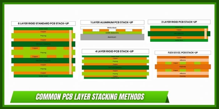 Common PCB Layer Stacking Methods
What are PCB Traces?
PCB traces are the copper paths on your board. They move signals and power between parts. You can think of them as internal routes. Every command, every response, travels through these lines. If traces fail, the circuit fails. That link is direct.
Why Trace Size Is Important
Trace width controls current flow. Wider traces carry more current. Narrow traces suit low-load signals. You must balance this carefully. If a trace is too thin, heat rises. If it is too wide, it wastes space. In PCB design, trace size shapes both safety and layout quality.
Challenges in PCB Traces
- Balancing Trace Width and Board Space – Board space is limited. You want wide traces for power. You also need room for signals. This creates tension. You adjust widths to fit both needs. The goal is steady current without crowding other paths.
- Preventing Interference and Short Circuits – Traces placed too close can interfere. Signals may couple. Noise increases. In worse cases, shorts appear. You avoid this with spacing rules and clean routing. Clear separation keeps signals predictable and stable.
- Traces in High-Speed and Compact Devices – High-speed designs push traces harder. Signals switch fast. Timing matters. In compact devices, paths become shorter and tighter. You must control length, spacing, and reference planes. When done well, traces stay quiet, even at high speed.
 PCB Traces
What are PCB Pads?
PCB pads are the landing points for components. This is where leads and terminations attach to the board. Pads are flat metal areas, usually copper. You rely on them for solder joints, signal flow, and part stability. Depending on the assembly method, there are various types of PCB pads such as Surface Mount (SMT) and Through-Hole pads. If a pad fails, the connection fails.
Why is Pad Material Important?
Pad material affects both soldering and reliability. Copper is the common choice. It conducts electricity well and handles soldering heat. When you heat the joint, the pad must stay intact. Weak material leads to lifted pads or cracked joints. Good copper pads keep connections stable over time.
Pad Stack Elements
- Via – A via is a plated hole. It moves a signal from one layer to another. You use vias to connect surface traces to inner layers. Without them, multilayer routing would stop quickly.
- Aspect Ratio – Aspect ratio compares hole depth to hole diameter. A high ratio means a deep, narrow hole. This is harder to plate. You must keep ratios within limits to ensure reliable copper coverage.
- Capture Pad – The capture pad surrounds the drilled hole. It connects traces to the hole plating. This pad holds the electrical link in place. If it is too small, joints weaken.
- Clearance Pad – The clearance pad is an opening in a plane layer. It keeps the hole isolated from that plane. You need this gap to prevent short circuits. It is also called an antipad.
- Hole Shadow – Hole shadow accounts for drill movement. It is slightly larger than the hole itself. You use it to calculate safe spacing to nearby copper. Ignoring this can reduce insulation margins.
- Plane Layer – A plane layer is a solid copper layer. It often carries ground or power. Pad stacks interact with planes through clearance pads. This control keeps currents predictable.
- Annular Ring – The annular ring is the copper left around the hole. It gives room for plating and trace entry. A healthy ring improves solder strength. Too small, and failures become more likely.
- Breakout – Breakout happens when the hole shifts outside the capture pad. This reduces copper support. It can weaken the joint or spacing. You avoid this with proper pad sizing and drilling control.
- Non-Functional Pads – Non-functional pads sit on inner layers with no connection. They once helped with plating balance. Today, they are often removed. This improves signal behavior and simplifies fabrication.
PCB Pad Placement
PCB pad placement feels like puzzle planning. You place each pad where the component expects it. Even a small shift can cause trouble. Pads must line up with leads, holes, and solder joints. When alignment is right, current flows without resistance. Power moves cleanly through the PCB pads.
At the same time, pads hold parts firmly in place. Loose parts lead to weak joints. Weak joints fail early. Pads also help spread heat. Warm parts pass heat into the copper, then into the board. This keeps temperatures steady. When you place pads with care, the whole circuit stays stable.
 PCB Pads
Partner with PCBMay: Professional PCB Production Supplier
With over 20 years of dedicated expertise in PCB manufacturing, PCBMay possesses the capability to produce your complex designs.
Our process capabilities, covering critical aspects such as layer count, trace width, and pad size, ensure the precision your project demands.
Precision Layer Count & Stackup
- Standard Range: 1–20 layers
- High-end Capability: 22–40 layers (supports HDI, high-speed communication, and mission-critical aerospace/defense boards)
High-Precision Line Width & Spacing
We support ultra-fine to heavy-copper trace designs (1/2OZ–10OZ copper weight) with industry-leading precision:
- Inner Layer: 3/3mil line width/spacing (1/2OZ copper) up to 12/27mil (10 OZ copper)
- External Layer: Min. 3.5/4mil line width/spacing (1/3OZ copper) up to 14/35mil (10OZ copper)
High-Reliability Pad Specifications
| Pad Type | Typical Size / Tolerance |
| Laser-Drilled Via Pads | 10 mil for 4 mil laser vias. 11 mil for 5 mil laser vias. |
| Mechanical-Drilled Via Pads | 16 mil pad for 8 mil mechanical drills. |
| BGA Pads | Standard: HASL 10 mil, LF HASL 12 mil, other finishes 10 mil. Advanced: 7 mil pads with flash gold for tight BGA layouts. |
| BGA Pad Tolerance | Standard: ±1.5 mil for pads ≤10 mil, ±15% for pads >10 mil. Advanced: ±1.2 mil for pads ≤12 mil, ±10% for pads ≥12 mil. |
Quality You Can Trust
- We strictly follow to IPC Class 2/3 standards and hold ISO, UL, REACH, and RoHS certifications.
- Every board undergoes 100% E-test, AOI, ICT, and flying probe testing to ensure your design’s precision is preserved from stackup to shipment.
Send your Gerber files for a FREE design-capability matching review and detailed quotation within 24 hours.
 PCB Layers, Traces, and Pads
Conclusion
PCB layers, traces, and pads are fundamental. Each element has a unique function. Layers build the structure. Traces carry signals. Pads provide connections. Understanding these components is key. It lets you design robust, high-performance boards. Consider stackup methods carefully. Pay attention to trace sizing and placement. This avoids common issues. Your design will thrive with this knowledge.
Frequently Asked Questions
Can You Put A Via On A Pad?
Yes. This is called “via-in-pad.” It is commonly used in high-density (HDI) designs and for BGA components with tight spacing (0.5 mm or less). It saves space by eliminating the need for extra trace routing.
How To Check PCB Traces?
You can check a trace with a digital multimeter. Set it to continuity mode. Place one probe at each end of the trace. If the meter beeps, the trace is intact. If there is no sound, the trace is broken or properly isolated.
How Many Layers Can A PCB Have?
The number of layers depends on circuit complexity and manufacturing limits. Simple designs often use one or two layers. More complex products need more layers for routing and power control. At PCBMay, standard production supports up to 20 layers, while advanced builds can reach 40 layers.
Can I Design My Own PCB With Custom Layers?
Yes, you can design your own PCB with a custom layer stack. You select layers based on signal, power, and layout needs. If you are new, start with a single-layer or double-layer board. As designs grow more complex, extra layers help increase density and routing flexibility.
How Do Traces And Vias In PCB Design Impact Performance?
Traces and vias control how signals move through your board. Traces that are too narrow can cause resistance and heat issues. Vias connect different layers and enable complex routing. Poor sizing or placement can lead to signal loss and reliability problems. Proper design improves overall board performance.
