
Top Partners Logo




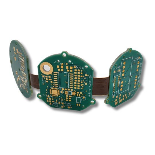
Why Choose PCBMay for Wearable Heart Rate Monitor PCBs?
- Ultra-Thin & Flexible Form Factors: We utilize advanced Rigid-Flex and HDI (High-Density Interconnect) technologies to ensure your heart rate monitor fits comfortably into sleek, ergonomic wearable designs without sacrificing performance.
- Superior Signal Integrity: Our precision manufacturing supports strict impedance control, essential for capturing low-voltage bio-signals and ensuring accurate, noise-free heart rate data during physical activity.
- Optimized Low Power Performance: Tailored for battery-operated devices, we support high-efficiency materials and specialized copper weights that help extend the battery life of continuous monitoring wearables.
- Medical-Grade Surface Safety: We offer medical-grade surface finishes like ENIG (Electroless Nickel Immersion Gold) and specialized solder masks that ensure long-term stability and safety for devices in close contact with human skin.
- Durability Against the Elements: With support for advanced conformal coatings, our PCBs are built to resist moisture, sweat, and environmental contaminants, ensuring the device remains functional throughout rigorous daily use.
What is a Wearable Heart Rate Monitor PCB?
A Wearable Heart Rate Monitor PCB is a precision-engineered circuit board manufactured to capture, process, and transmit vital biometric data from the human body. As the central nervous system of fitness trackers and medical-grade wearables, these boards manage the complex interaction between optical sensors, microcontrollers, and wireless modules. Unlike standard electronics, these PCBs must maintain high signal sensitivity while being subjected to constant movement, body heat, and varying moisture levels. They are the core technology inside smartwatches, chest straps, and clinical patches, ensuring that every heartbeat is recorded with medical-grade accuracy.
These boards are essential for a wide range of devices, including high-performance fitness wearables, remote patient monitoring systems, and specialized athletic diagnostic tools.
At PCBMay, we combine specialized fabrication techniques to build boards that meet the exacting demands of the wearable tech industry. Our craftsmanship ensures that ultra-compact form factors maintain structural and electrical integrity during long-term use. We utilize advanced HDI technology with 3 mil trace/space capabilities and 01005 component precision to pack high-level functionality into small footprints. By leveraging high-grade flexible and rigid-flex materials, we deliver robust solutions that handle the mechanical stresses of wearable applications effectively. Every board is produced under stringent ISO 13485 standards to ensure your devices provide stable, long-term performance in the field.
Ready to bring your next health-tracking innovation to life? Contact our engineering team to discuss your specifications or get a custom quote today!
PCBMay Service Advantage for Your Wearable Heart Rate Monitor PCB
PCBMay offers specialized, medical-grade PCB solutions tailored for the medical PCB manufacturing and medical PCB assembly of sophisticated wearable health technology. We provide ultra-compact, reliable, and high-performance boards designed to meet the rigorous demands of continuous biometric monitoring and patient safety.

Our rapid fabrication services help you accelerate your R&D iteration and sample validation, supporting faster project verification and clinical trial progress for wearable health devices.

Our engineering team performs professional DFM/DFA manufacturability reviews tailored for HDI and rigid-flex structures. We ensure your stackup is optimized for signal integrity and mechanical flexibility, identifying potential issues before production begins.

As a total solution provider, we manage the entire lifecycle from sourcing specialized medical-grade components to precision SMT (Surface Mount Technology) assembly. We are equipped to handle the delicate placement of miniature sensors and micro-BGAs essential for wearable tech.

Our production lines comply strictly with ISO 13485 medical quality standards and IPC Class 3 requirements. With full process traceability and advanced ESD protection, we ensure your wearable devices meet global regulatory and safety standards.
Wearable Heart Rate Monitor PCB Case Studies
The following case studies show real-world production examples of wearable heart rate monitor PCBs designed for ultra-compact, precise biosensing applications.
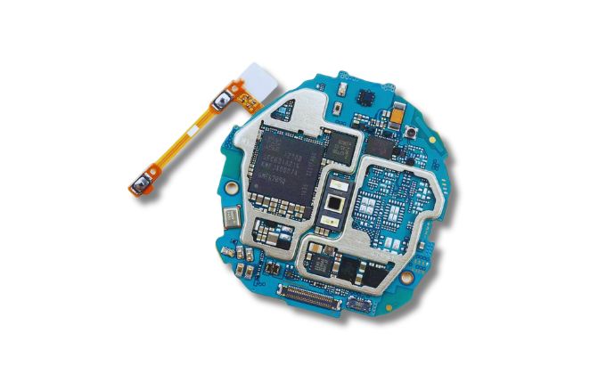
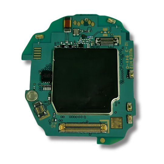
PCBMay provides specialized turnkey services for high-performance health wearables. The customer needed a compact rigid-flex PCB solution for wearable wrist devices with long-term bending endurance. The primary challenge was achieving high-density component integration while maintaining mechanical durability during constant user movement. We solved it with 3-mil fine-line HDI fabrication and a customized rigid-flex stackup to fit slim wearable structures. The final ISO 13485-certified solution ensured exceptional signal integrity and long-term reliability for accurate, 24/7 heart rate monitoring.
Technical Specifications:
- Layer Count: 4 layers (rigid section)
- Material: High-Tg FR-4 (Shengyi S1000H, Tg 180℃) / Polyimide (PI) rigid-flex stackup
- Board Thickness: Rigid section: 0.8mm; Flexible section: 0.1mm
- Copper Thickness: 1 oz (35µm)
- Min Line/Spacing: 3mil/3mil
- Surface Finish: ENIG
- Component Assembly: Supports 01005 SMD components, fine-pitch high-density assembly
- Additional Service: Full turnkey PCBA with component sourcing and functional testing
- Certifications: ISO 13485 Certified, IPC Class 2 Qualified, RoHS Compliant
- Application: Wearable Heart Rate Monitor Smartwatches
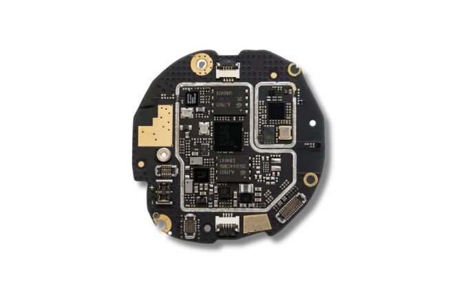
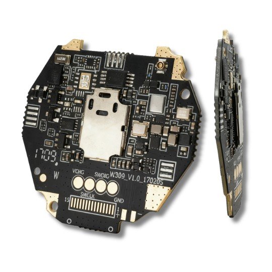
PCBMay provides expert turnkey assembly for the main control units of advanced medical wearables. The customer needed an ultra-thin 6-layer high-density PCB for medical-grade biosignal precision monitoring. The key challenge was suppressing EMI noise and preserving clean biometric signals in a 0.6mm ultra-thin slim profile. We addressed this by using high-performance Isola 370HR materials, implementing precision shield can soldering, and utilizing 01005 fine-pitch assembly. The final ISO 13485-certified solution ensured high-speed, reliable data collection for 24/7 heart rate monitoring.
Technical Specifications:
- Layer Count: 6 layers
- Material: Isola 370HR (Tg 180℃) with black solder mask
- Board Thickness:6mm
- Copper Thickness: 1 oz (35µm)
- Min Line/Spacing: 3mil/3mil
- Surface Finish: ENIG
- Component Assembly: Supports 01005 SMD components, fine-pitch high-density assembly with shield cans soldering
- Certifications: ISO 13485 Certified, IPC Class 2 Qualified, RoHS Compliant
- Application: Wearable Heart Rate Monitor Smartwatch Main Control Units
Testimonials
We rely on PCBMay for our wearable heart rate monitor PCBs. Their expertise in high-density HDI and rigid-flex technology allowed us to reduce our device footprint by 30% while maintaining incredible signal accuracy during high-intensity workouts. Their boards are the heartbeat of our product line.
 David AristhoneLead Hardware Architect, FitCore Innovations
Wearable health tech is constantly exposed to sweat and movement. PCBMay provides PCBs that withstand daily environmental stress while maintaining perfect electrical integrity. Their ISO 13485 certification and rigorous AOI testing give our team total confidence that our patient monitoring patches are both safe and reliable.
 Elena RodriguesDirector of Biometric Systems, VitalLink Wearables
Related Product

We manage the entire manufacturing process, from sourcing specialized biometric sensors to final functional testing. Our all-in-one approach for wearable heart rate monitor PCBAs streamlines your production timeline while ensuring every unit meets the highest medical standards for signal accuracy and user safety.

Our flagship offering for mission-critical health applications. These boards deliver stable, 24/7 performance in remote patient monitoring and clinical diagnostic tools, supported by full process traceability and ISO 13485 compliance.

The foundation of modern wearable technology. By utilizing microvias and fine-pitch routing, we enable the integration of complex microcontrollers and wireless modules into ultra-compact footprints, enabling sleek, comfortable wristbands and chest straps.

Essential for the ergonomic demands of wearable devices. Our thin, lightweight, flexible circuits allow the PCB to contour to the human body, providing the mechanical durability needed to withstand constant bending and movement without circuit fatigue.

The perfect solution for sophisticated wearables that require both a stable mounting surface for sensors and a flexible tail for battery or display connections. This hybrid technology eliminates the need for bulky connectors, saving critical space and weight in portable designs.

We offer advanced fabrication of up to 40 layers. The superior signal shielding and dedicated ground planes of our multilayer boards ensure that delicate heart rate data and low-voltage bio signals are perfectly insulated from electromagnetic interference and digital noise.
The Crucial Role of PCBs in Wearable Devices
PCBs, or Printed Circuit Boards, are a core component in wearable technology. They provide the structure and electrical support needed to create small and compact devices for health tracking. A wearable heart rate monitor PCB ensures that the components are highly integrated and fit into the small footprints of fitness devices. These boards provide the mechanically miniaturized platform integrating electrical and electronic components, ensuring everything works, and power devices operate efficiently. You can create compact and performance-oriented smart watches using a high-density design layout.
Why PCB Innovation Matters for Wearable Health Monitors
Innovation allows health trackers to be compact and lightweight while achieving medical precision. Modern manufacturing processes deliver higher power efficiency and eco-friendly material compliance for long-term wearable applications. As a result, you don’t have to give up comfort or battery life to receive continuous monitoring of vital signs. It is modern manufacturing techniques that make these high-tech tools reliable and affordable.
- Driving Miniaturization and Comfort: High-density layouts and thinner materials allow you to place your advanced sensors into smaller ergonomic footprints for a sleeker and more comfortable fit.
- Ensuring Medical-Grade Data Accuracy: Advanced shielding and specialized materials in medical-grade wearable PCB assembly minimize signal noise, which results in medical-grade data precision.
- Improving Power Efficiency: By adopting optimized manufacturable layout rules and deployment of thin-film batteries, we achieve a low power system efficiency in wearable devices to utilize the maximum energy. It powers the monitor throughout the long workout sessions and sleep cycles.
- Supporting Flexible Form Factors: Smartwatch manufacturers are building flexible PCBs and circuits that bend like your body, preventing internal damage during movement.
Key Design Considerations for Heart Rate Monitor Band PCBs
The boards are designed with size, signal clarity, and mechanical flexibility in mind. To ensure safe and long-term use of the device, you have to use power efficiently and thermally manage it. Taking these into account allows the creation of a high-performance monitor that suits the user’s daily life. Using a medical-grade wearable PCB assembly process is critical for meeting such strict requirements.
- Miniaturization and Form Factor: Having multi-layer designs and micro-vias allows miniaturization and generates lightweight components for fixing complex electronics. Your device stays thin and comfortable without compromising on any necessary sensors.
- Flexibility and Durability: Creating a smart watch flex PCB design with a polyimide substrate will make a circuit that fits the body. This method avoids trace cracking, allowing your device to maintain mechanical stability during constant movement.
- Signal Integrity and Noise Reduction: Grounding ensures that sensitive analog information doesn’t get interfered with by noise. Noise can easily mess with any type of detection system. Isolating the biometrics from the digital interference gives clean and reliable heart rate readings.
- Power Management and Efficiency: Boosting battery performance for wearable health trackers includes selecting low-power parts in addition to using layout to eliminate current leakage. Power-efficient voltage regulation will keep the device active for days to improve the user experience.
- Thermal Management: The deliberate arrangement of heat-dissipation structures and thermal vias can reduce device temperature at the skin level. By keeping the components cool, the performance is not hampered while ensuring the safety of users and the reliability of components over the long haul.
- Biocompatibility and Environmental Resistance: Eco-grade substrate materials and waterproof conformal coating protect circuits from moisture and sweat for fitness wearables. These selections shield sensitive electronic pieces from moisture and sweat while avoiding irritation
Advanced PCB Materials: Durability & Eco-Friendly Wearable Compliance
Modern wearables are designed from special materials that do not rub off due to their constant movement and exposure to the atmosphere. To ensure both user comfort and device reliability, you must prioritize skin-contact safe PCB materials and flexible substrates. With these smart options, the circuitry shall not malfunction, and the user shall not get an allergy. Utilizing these materials, you can create thinner and more robust health monitoring devices.
- Flexible Substrates: Polyimide substrates let your device bend back and forth without cracking or losing electrical integrity.
- Biocompatibility: Eco-friendly and non-irritating base materials ensure safe wearable application and long-term wearing comfort.
- Conductive Inks: Silver nanoparticle inks allow ultra-thin and lightweight circuits that perfectly match the body contours.
- Sustainability: Eco-friendly components help you design health technology with a significant reduction in the environmental footprint.
Manufacturing Processes: Ensuring Precision and Reliability
To ensure its efficiency and durability, a wearable heart rate monitor PCB needs high accuracy. We carry out every process from material preparation to testing to enable your device to stand up to daily use without issues. Our techniques protect signal integrity in compact, flexible geometries. This rigorousness prevents you from failing your body-worn health trackers.
Substrate Preparation and Imaging
The process begins with choosing flexible polyimide and printing your circuit design using light. The core material is cleaned properly before a thin copper layer is added. UV light and photoresist are then employed to fix the exact traces. The photolithography procedure transfers patterns needed for small devices. Implementation of accurate imaging ensures the functionality of rigid-flex PCB for fitness trackers.
Etching and Multi-Layer Lamination
We use a chemical process to eliminate extra copper, retaining only the required circuit traces. In the case of complex devices, we press layers of each portion separately. The layers are bonded through an insulating adhesive at high temperature and pressure. Perfect alignment is crucial at this lamination step. This precision stops electrical shorts and allows your wearable to communicate perfectly.
Drilling and Plating
Advanced lasers and CNC machines puncture small openings to enable circuit layers to connect electrically. Vertical signals and mount points for tiny components are provided by these vias. We proceed to chemically plate the interior walls with copper to ensure good connections. A uniform type of plating process is necessary for ensuring reliability in the long run. This step ensures that there is a perfect electrical connection throughout the device.
Solder Mask and Surface Finish Application
Accidental short circuits and oxidation are prevented by the application of a protective polymer coating on copper traces. This solder mask protects the circuit board but leaves pads for your components unmasked. Subsequently, we utilize a specific surface finish like ENIG on these exposed areas. This coating safeguards the bare copper and guarantees superior solderability. Your board is now ready to receive its electronics.
Component Assembly (PCBA)
The PCB assembly makes a health monitor functional from the bare board for medical-grade use. Automated machines quickly and accurately position small components onto the solder paste. The board is then sent through the reflow oven, which melts the paste and bonds the joint. Our process for flexible boards employs low-temperature soldering techniques. The intricate assembly procedure used prevents overheating of fragile components.
Testing and Quality Control
Rigorous testing at multiple stages guarantees your completed board meets all strict functional specifications. We use optical inspections to catch manufacturing defects before they become real problems. In-circuit tests verify that every component is properly connected and functioning. We also simulate real-world environmental stress, like humidity and temperature changes. This strict quality control ensures your wearable survives intense daily activities.
Future PCB Technology for Wearables: Smaller, Smarter, and More Efficient
A new wearable heart rate monitor PCB will possibly be based on extreme miniaturization and other enhanced performance. To optimize comfort, you need to pack complex functionalities into tiny footprints. Online layouts focus on energy efficiency and fast signaling. These inventions ensure your health monitors work smoothly.
Miniaturization & HDI Technology
Your best option for miniaturizing wearables is high-density interconnect (HDI) technology. You fabricate tighter pitches, miniature vias, and finer traces to squeeze in functionality. HDI can make trace widths down to 50 µm. This develops a mini PCB layout for ring sensors not wider than a coin. You keep highly effective operation in ultra-small designs.
Flexible Hybrid Electronics: Merging Comfort with Functionality
Adaptable hybrid electronics combine everyday user convenience with fast data processing. A 50-ohm impedance control provides fast, accurate medical feedback. Tracking important metrics, such as blood oxygen, prevents data loss. They also consume 30% less energy. When you optimize battery life in your wearable health tracker, the device runs for days.
PCB Trends in Medical Devices: Meeting Stringent Standards
Medical devices require complete reliability in order to comply with regulatory specifications and safeguard patients. Your wearable monitor’s circuit failure may produce unsafe inaccuracies. Medical-grade wearable PCB assembly requires an assembly that is highly accurate and secures data. Following these strict standards, the current top trends have been formed.
- Adopting Multi-Layer Boards: To manage complex medical capabilities in a compact area, you need multi-layer types. You can densely pack components on the boards that contain 8 or more layers. This design maintains signal integrity when your device analyzes heart rate and motion data concurrently.
- Integrating Wireless Connectivity: Incorporating the antenna directly into the circuit board is done utilizing a Bluetooth LE antenna design for wearables. The device will be extremely compact and allow simultaneous data uploading at 2 Mbps.
Manufacturing Challenges & Solutions for Wearables
The production of flexible boards is usually accompanied by high cost and quality hurdles. Balancing high performance and battery life optimization within small footprints is a challenge for wearable health trackers. You can predict thermal errors early on and solve these problems using automated and AI tools. Affordable and effective Medical Grade Wearable PCB Assembly solutions for your project.
Opportunities in Personalized Healthcare.
As personalized medicine continues to grow, the demand for highly customized circuit designs increases. Wearables can now be customized to monitor specific conditions, such as sleep apnea and arrhythmia. In short, these boards make the medical device affordable while ensuring that the device does not lose its effectiveness. Being able to customize enables you to meet individual patient needs with high-precision electronics. The transition to niche medical applications is changing the future of wearable technology.
Case Studies: Successful Wearable Heart Rate Monitor Band Projects
PCBMay’s precision manufacturing has solved various real-world issues in the wearable-related projects we successfully completed. Our job is to decrease form factor and improve product robustness through material science and layout optimization. Our collaborations highlight our commitment to reliable, high-density circuitry in the health and fitness sector. When you choose PCBMay, you have a partner who can deal with the demanding medical standards and mass-market cost constraints.
| Project Name | Client Challenge | PCBMay’s Contribution | Key Outcome |
| Ultra-Slim Fitness Tracker | Achieving extreme miniaturization and flexibility for a sleek, discreet design. | Developed a 0.3mm multi-layer flexible PCB with advanced signal integrity features. | Reduced device size by 25% while improving wearer comfort and biometric accuracy. |
| Rugged Outdoor HR Monitor | Ensuring durability and water resistance for use in extreme environmental conditions. | Applied specialized waterproof PCB coating for fitness wearables and robust mounting. | Achieved IP68 rating, ensuring reliable performance during swimming and outdoor sports. |
| Medical-Grade ECG Band | Meeting ISO 13485 standards for high precision and low signal noise. | Manufactured optimized analog routing and professional EMI shielding for medical-grade wearable PCB assembly. | Passed rigorous clinical certifications for use in professional medical diagnostics. |
| Cost-Optimized Wellness Band | Balancing high-end performance with competitive pricing for the mass market. | Implemented intelligent panelization and cost-effective material selection strategies. | Realized a 15% cost saving per unit, driving significant growth in market share. |
Why Partner with PCBMay for Wearable Heart Rate PCBs
PCBMay offers ultra-thin multi-layer wearable PCBs that are certified compliant with strict global medical safety standards as well as IPC Class 3. We provide professional contract manufacturing services for biometric monitors with batch, component, and process traceability at all stages. We provide one-stop medical-grade PCB fabrication and PCBA assembly services. If you are looking for a compliant and experienced medical electronic contract manufacturer, partner with us. Send your specifications today for a customized solution and competitive quote.
Flexible and rigid-flex PCBs are ideal as they can easily change shape to fit the body and endure endless movement. In order to make sure that the device is lightweight and durable, you should use Polyimide substrates, which will also protect the sensors.
It is possible to employ multilayer flexible designs with four or more layers to fit advanced biometric components. HDI technology and micro-vias help these boards stay slim while performing complex tasks and functions.
Wearables rely on small batteries, so the PCB layout should minimize energy waste to keep the gadget alive for days. To maximize battery life in wearable health trackers for constant monitoring.
Signal noise reduction in optical heart rate sensors can be done by grounding and isolating components within the device. It helps protect sensitive analog signals from digital noise for medical precision in diagnostics.
The optimal thickness is usually 0.33 oz to 0.5 oz so that traces do not crack when repeatedly bent. Your wearable heart rate monitor PCB becomes more fatigue-resistant and more flexible with thinner copper.