

Top Partners


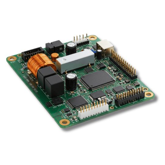
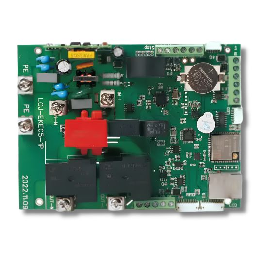
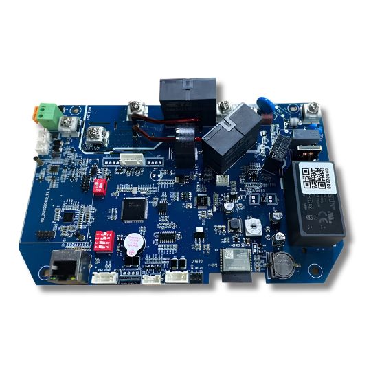
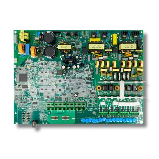
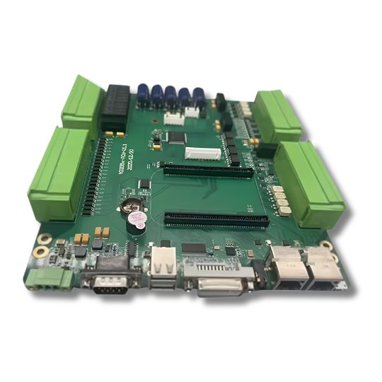

High-Performance EV Charger PCB Features
- Robust High-Voltage & Isolation Performance: We make EV charger PCBs in line with creepage and clearance standards and use high-CTI materials for EVSE. Our professional high-voltage manufacturing processes lower risks of electric arcing and leakage current within compact charger enclosures.
- Complete SMT & THT Production Capacity: We are equipped with 8 dedicated SMT and THT production lines to support fully automated component placement and through-hole insertion. Excellent board flatness guarantees consistent, reliable soldering for both standard parts and high-power components.
- Superior Thermal Management Solutions: Backed by rich experience in thermal control, we maintain an ample inventory of high-Tg laminates. We also support heavy copper PCBs up to 10 oz, plus embedded copper coins, busbars, and thermal vias. These proven technologies deliver excellent thermal performance for all types of EV charger PCBs.
- Impedance Control & Signal Integrity: Our engineering team ensures tightly controlled impedance lines for critical onboard communication networks (such as CAN bus, RS485, OCPP, and Ethernet protocols). This maintains crystal-clear data transmission between the vehicle’s BMS and the charger’s primary controller, eliminating signal degradation caused by nearby high-voltage switching fields.
- Rigorous Testing & Automated Inspection: Every batch undergoes comprehensive testing, including Flying Probe testing, and X-ray inspection for high-density BGA packages. For power modules, we perform strict high-voltage isolation (Hi-Pot) testing and thermal stress analysis to guarantee zero-defect field performance under extreme field stresses.
- Waterproof Outdoor Protection: We provide optional conformal coating services to safeguard finished PCBs against moisture, dust, and corrosion. This ensures stable and long-term operation for outdoor EV charging stations.
What is an EV Charger PCB?
An EV Charger PCB is a heavy-duty circuit board specifically manufactured to handle high power levels and regulate energy flow within Electric Vehicle Service Equipment (EVSE). It serves as the primary backbone for both AC Level 2 chargers and DC fast charging systems, safely monitoring communication protocols, managing critical thermal dissipation, and conducting high-current loads to the vehicle battery. Unlike standard consumer electronics, these rugged boards feature thick copper layers, optimized dielectric barriers, and standard creepage and clearance to prevent electrical arcing, minimize power loss, and protect sensitive control microprocessors from high-frequency electromagnetic interference (EMI). They are indispensable components for green energy companies and infrastructure developers building residential charging stations, commercial fleet hubs, and highway fast-charging networks.
PCBMay specializes in manufacturing high-reliability EV charger PCBs and complete PCBA services. Please submit your Gerber and BOM files now, and our technical team will give you a free DFM review and quick quotation.
PCBMay Service Advantage for Your EV Charger
PCBMay offers commercial manufacturing and assembly of your EV charger PCB. Our mature production capabilities fully meet high-voltage standards and severe thermal loads of modern EV charging systems. We excel in thick copper plating, electrical isolation, and professional thermal dissipation for next-generation charging modules.

Speed up your development timeline with our fast-turn fabrication. We offer quick-response prototype runs for complex, high-power boards, helping you complete electrical safety and communication protocol testing without production delays.

We offer a manufacturability review for free before production. Before formal manufacturing begins, our engineers inspect your design to proactively determine manufacturing bottlenecks, component spacing issues, or thermal problems you may encounter, and help you avoid any extra manufacturing costs.

We handle the entire project from beginning to end. This includes complicated processes of custom PCB substrate procurement and full parts procurement, precision assembly of large SMT devices, and heavy parts THT connectors.

As all boards were processed to meet ISO 9001 and IPC Class 2/3 standards, they performed very well under repeated high currents. Each and every batch is produced with full production traceability, high voltage isolation testing documentation, and thermal verification report.
Energy Storage PCB Case Studies
The following case studies showcase PCBMay’s real-world production examples of EV Charger PCBs. These boards are engineered for exceptional thermal dissipation and ultra-high power throughput, ideal for demanding DC fast-charging infrastructure and high-power commercial fleet charging networks worldwide.

PCBMay manufactured this 6-layer central controller for a commercial EV charging network. It delivers safe power communication and highly accurate system telemetry. The main challenge was routing ultra-dense circuitry alongside sensitive high-speed data lines. We efficiently managed the assembly of standard 0402 SMD components without causing signal interference. To achieve this, we utilized premium high-Tg Isola 370HR base material. The layout features precise 4mil trace spacing and uniform 2oz copper. This sturdy 1.6mm thick profile maintains excellent thermal stability and blocks high-frequency noise. Finished with oxidation-resistant ENIG, this IPC Class 3 certified board guarantees flawless long-term operation.
Technical Specifications:
- Layer Count: 6 Layers
- Material: Isola 370HR
- Board Thickness:6 mm
- Copper Thickness: Outer Layers: 2 oz / Inner Layers: 2 oz
- Min Line/Spacing: 4 mil / 4 mil
- Surface Finish: ENIG
- Placement Accuracy: ±0.035mm
- Certifications: ISO 9001, IPC Class 3 Qualified, RoHS Compliant
- Application: Commercial EV Charging Station Central Controller

PCBMay manufactured this 4-layer power module for a commercial EVSE network provider. It delivers safe high-amperage AC routing and intelligent safety monitoring. The main challenge was processing heavy power distribution paths alongside fine-pitch microcontrollers. We efficiently managed the assembly of heavy-duty THT terminals and large relays without causing operational interference. To achieve this, we utilized premium high-Tg Shengyi S1000-2M base material. The layout features reliable 8mil trace spacing and robust 3oz outer copper. This thickened 2.0mm profile handles intense localized heat spikes and completely eliminates electrical arcing risks. Finished with strong Lead-Free HASL, this IPC Class 3 certified board guarantees flawless long-term outdoor operation.
Technical Specifications:
- Layer Count: 4 layers
- Material: Shengyi S1000-2M
- Board Thickness:0mm
- Copper Thickness: 3oz (Outer layers) / 2oz (Inner layers)
- Min Line/Spacing: 8mil/8mil
- Surface Finish: Lead-Free HASL
- Placement Accuracy: ±0.035mm
- Certifications: ISO 9001 Certified, IPC Class 3 Qualified, RoHS Compliant
- Application: 22kW AC EVSE Main Power & Intelligent Control Module
More about PCBMay
Here you can review our capabilities, watch related videos, and view factory images.
- PCB Manufacturing Capabilities
- PCBA Assembly Capabilities
- Video
- PCB & PCBA Factory
| Capability Feature | Rigid PCB | Flexible PCB | Rigid-Flex PCB | Metal Core PCB |
| Max Layer Count | Up to 40 Layers | Up to 8 Layers | Up to 20 Layers | 1–4 Layers (Single/Double/Multi) |
| Base Materials | FR-4, High-Tg, Rogers, PTFE, IS410 | Polyimide (PI), FCCL (Adhesive/Adhesiveless) | FR-4 + PI, No Flow PP | Aluminum, Copper, Iron |
| Max Copper Thickness | Up to 100 oz | Up to 3 oz | Up to 5 oz | Up to 240 um (~7 oz) |
| Board Thickness Range | 0.2 mm – 10.0 mm | 0.05 mm – 0.8 mm (without stiffener) | 0.3 mm – 4.0 mm | 0.3 mm – 5.0 mm |
| Max Board Size | 1100 mm × 500 mm | 9 inches × 23 inches | 406.4 mm × 736.6 mm | 1500 mm × 600 mm |
| Min. Trace / Space | 3.0 / 3.0 mil | 3.0 / 3.0 mil | 3.0 / 3.0 mil | 0.1 mm (~4 mil) |
| Surface Treatments | HASL, ENIG, ENEPIG, Hard/Soft Gold, OSP, Silver/Tin | HASL, ENIG, ENEPIG, Gold, OSP, Silver/Tin | HASL, ENIG, ENEPIG, Gold, OSP, Silver/Tin | LF HASL, ENIG, OSP, Chemical Silver/Tin |
| Thermal Conductivity | / | / | / | Up to 5.0 W/mK |
| Assembly Parameter | PCBMay Production Capability |
| Minimum Order Quantity | ≥ 1 Piece (From quick prototypes to mass production) |
| Quality Standards | IPC-A-610 Compliance (Class 2 and Class 3) |
| Production Lead Time | 24-hour fast-turn available; 3–4 days for standard prototypes |
| Board Size Limits | Min: 50 mm × 50 mm / Max: 510 mm × 460 mm |
| Compatible Board Types | Rigid PCB, Flexible PCB, Rigid-Flex, Metal Core (Aluminum) |
| Minimum Component Package | 01005 (0.4 mm × 0.2 mm) |
| BGA Assembly Limits | 0.14 mm Ball Diameter, 0.2 mm Ball Pitch |
| Assembly Accuracy | ±0.035 mm (±0.025 mm fine pitch) Cpk ≥ 1.0 |
| Assembly Types Supported | Surface Mount (SMT), Through-Hole (DIP), Mixed Technology |
| Component Sourcing | Full Turnkey, Partial Turnkey, or Kitted/Consigned |
| Quality Inspection Systems | Visual Inspection, Automated Optical Inspection (AOI), 3D X-Ray |
| Daily SMT Production Capacity | 3 Million to 4 Million Soldering Pads per day |
| Daily DIP Production Capacity | 100 Thousand Pins per day |
| Conformal Coating Options | Acrylic (AR), Silicone (SR), Polyurethane (UR), UV Curable |
PCB Factory


PCBA Factory


Testimonials
The ultra-dense residential charging modules required tight PCB space constraints, required strict thermal dissipation requirements, and had to meet stringent electrical safety standards. PCBMay was our partner of choice for heavy copper material fabrication that passed all stringent high voltage insulation and arcing series of tests. Our ability to process the thick trace routing and true contact of large power terminal components and communication chips enabled our optimization of the use of hardware in our EV Charger PCB.
 Dennis VermondVP of Hardware Engineering / Director of Hardware Design
We collaborated with PCBMay for our next-generation public DC fast-charging networks, and their expertise in high-voltage circuit isolation and heavy copper plating is unmatched. Our charging units achieve flawless power distribution with zero voltage drops, thanks to the exceptional thermal management and precision heavy-gauge trace stackups they maintain across our complex EV Charger PCB designs.
 Michaela RuthPrincipal Power Infrastructure Engineer / Senior Systems Engineer
Related Product

We manage everything from sourcing high-voltage power components to final electrical safety and cell-balancing test procedures. Our all-in-one approach for EV power electronics streamlines your production timeline while ensuring every finished unit meets strict automotive and industrial standards.

The primary foundation of high-current charging electronics. We manufacture heavy copper PCBs with traces up to 10 oz. This thick copper structure effectively cuts down circuit resistance and thermal losses, making it ideal for high-load power conversion loops and rugged busbar paths.

A high-reliability functional platform for onboard power electronics and vehicle interconnection. Our automotive-grade PCBs are manufactured using high-Tg laminates with strict insulation boundaries to withstand continuous road vibrations, temperature fluctuations, and high-voltage stress.

The precision measurement engine for smart charging stations and commercial billing networks. Standard multi-layer isolation and precise impedance control shield sensitive data lines from EMI, enabling real-time data transmission and accurate power consumption.

We offer advanced fabrication up to 40 layers. The superior power shielding, optimized layer stackups, and high-voltage isolation of our multilayer boards allow sensitive microprocessors and logic lines to be perfectly insulated from high-frequency switching noise, preventing EMI corruptions.

Manufactured to bear heavy thermal loads from high-power charging modules. These boards feature specialized aluminum or copper bases to rapidly draw heat away from hot power switching transistors and rectifier circuits, maintaining optimal system efficiency.

Built with robust, heat-resistant materials to support reliable operation under continuous thermal stress. Perfect for dense charging enclosures and heavy-duty outdoor EVSE units, these boards prevent material degradation and structural expansion to ensure stable performance over long service lifetimes.
The Importance of EV Charger PCB Assemblies
The PCB assemblies in electric vehicle chargers are very crucial in managing the routing of high-power electricity on its way. They allow safe conversion of power from the source, regulate the output current, and monitor the system during every charging session. The complete structural integrity of your charging station and its functional safety comply with these boards. If this assembly is not optimized, it could lead to significant system downtime, damage to parts, or electrical faults.
Enhancing Safety
The most important requirement for any operational EV charger PCB assembly is safety. These specialized circuit boards have robust protection circuits that protect a malfunctioning hardware and vehicle from catastrophic electrical damage. Your system has high insulation barriers to prevent high-voltage arcing and destructive short circuits. In addition, the assembly disengages power through automatic shutdown when any parameters become excessive.
- Overcurrent and Overvoltage Protection: The vehicle is protected from heavy voltage and current spikes from the grid using fuses and surge arrestors.
- Thermal Management Systems: The temperature sensors monitor heat build-up continuously, then trigger cooling or throttle current.
- Grounding and Insulation Mechanisms: High-voltage paths are safely contained by making use of thick dielectric materials and also wide physical spacing.
- Fault Detection and Shutdown Procedures: Hardware and control logic can shut down power delivery within milliseconds when abnormal conditions are detected.
Improving Efficiency
Charging cycle efficiency is enhanced using optimized EV charger PCB assemblies that maximize total power transfer and minimize energy loss. Your board does this through the use of heavy copper tracking to lower electrical resistance and parasitic power losses. When you choose high-quality switching components, the thermal generation is as low as possible so that the charging station works coolly even at peak operation. The engineering improvements reduce your total operating costs and reduce the environmental impact of EV infrastructure.
Ensuring Reliability
Long-term reliability ensures your charging station withstands continuous outdoor use. We build these robust assemblies using rugged industrial-grade laminates. These materials can withstand heavy quantities of moisture, temperature fluctuations, and vibration. Our precise automated soldering and strict testing prevent early joint fatigue and structural delamination. This durable construction protects your infrastructure while reducing expensive field maintenance.
Advances in PCB Technology for EV Charging Systems
Recent developments in PCB manufacturing technology bring about key engineering innovations that enhance the performance of today’s EV charging networks. With these advanced techniques, your charging hardware can accommodate higher power transmission, while overall cabinet space can be drastically reduced. Utilizing advanced manufacturing processes, you can ensure the construction of smart, compact, and thermally stable EVSE.
- High-Density Interconnect (HDI) PCBs: HDI PCB technology employs microvias and fine line spacing to cram enormous computing power into very small board footprints. As a result, all your complex control microprocessors, communication modules, and also user interfaces work off a single layout with little signal delay.
- Flexible and Rigid-Flex PCBs: Combining rigid and flexible structures, rigid-flex circuits fit the complex form factors of EV chargers. They cut bulky wiring harnesses, minimize manual assembly errors, and prevent connector damage caused by mechanical vibration.
- Embedded Components and Advanced Materials: Embedding active and passive components inside inner layers increases the available surface area and greatly mitigates interference from high-frequency electromagnetic interference (EMI). The use of advanced high-temperature laminates helps prevent board delamination and improves thermal performance during heavy fast-charge operation.
EV Charger PCB Material
Choosing the right substrate means that your charging station can safely manage high electrical currents and high thermal loads. The maximum voltage, heat dissipation, and outdoor mechanical resistance of the board depend mainly on the selected base material.
- High-Tg FR4: This cost-effective foundation offers high thermal resilience for continuous operating heat. Reliable high-Tg options include Isola 370HR, Shengyi S1000-2M, and ITEQ IT-180A. It is the ideal choice for stable electrical insulation in standard AC charging station control circuits.
- Heavy Copper: Heavy copper layers provide a low-resistance heat path for extremely large high currents. This strong structure prevents trace burnout during high-power fast-charging.
- Rogers: The specialized ceramic-filled PTFE laminates by Rogers exhibit excellent high-frequency behavior and low loss. There is clear communication and no noise between the car and the charger controller.
- Ceramic PCB: The ceramic substrates have high thermal conductivity and exceptional high voltage electrical insulation. Their ultra-stable structure totally removes the risk of parasitic leakage in dense power modules.
Thermal Management Challenges in High-Power Charging
When multi-kilowatt rapid charging continues, many hundreds of amps pass through power electronics, generating substantial Joule heat losses) in internal copper tracking. If this amount of intense heat is not getting removed or dissipated efficiently and effectively, hot spots will quickly form that will age the material rapidly, degrade the solder joints of components, and pose serious hardware safety risks. To effectively mitigate these extremes in thermal load, a multidimensional manufacturing approach is required that integrates low-resistance power traces with high-conductivity physical heat sinking.
- Heavy Copper Technology: The use of 3 oz or heavier copper foil to minimize the trace resistance and, consequently, the heating generated within. This supports stable current-carrying capacity and improved joint reliability along high-power paths.
- Thermal Vias Array: A thermal vias array refers to dense arrays of plated through-hole thermal vias placed within the component footprint to draw heat away from the component to the opposite side of the board. The design implements heat transmission quickly to the internal dissipating planes to maximize the cooling surface area.
- Metal Core PCBs (MCPCBs): Metal Core PCBs are heavy-duty power modules that use specialized aluminum or copper substrates instead of glass fiber, providing unmatched physical thermal conductivity. These metal base layers effectively direct concentrated system heat away from components and into either external chassis heat sinks.
- Embedded Copper Coins: By press-fitting solid copper blocks directly within the board stackup, ultra-low thermal resistance paths are established under large power switching transistors. When you are dealing with high-stress DC-DC converter boards or heavy-duty contactor control systems, this targeted technique gives fast thermal relief.
Key Components of EV Charging Systems
EV charging stations rely on integrated hardware modules to safely regulate power and vehicle communications. Your advanced circuit boards act as the foundation linking these components together. They unite these separate systems into a highly responsive network. Industrial tolerances are used when building these boards to ensure smooth power conversion and fast telemetry.
- Power Modules: Power modules are basically sub-circuits that convert AC from the grid to different levels of voltage required to charge the battery of the vehicle.
- Communication Modules: The communication modules are the data networks that ensure an uninterrupted, noise-free communication and handshake of the protocol between the internal computer of the electric vehicle and the station controller.
- Control Units: Control units are intelligent microprocessors that perform the function of the overall brain of the station and control the real-time execution of the charging cycle.
- Safety and Protection Circuits: This fast-acting isolation network permanently monitors the operating parameters of the HVDC system to instantaneously isolate high voltage faults and eliminate the risk of predominant or hazardous failure of the system.
Best Practices for EV Charger PCB Assembly
Implementing automotive-grade manufacturing protocols ensures your EV charger PCBs achieve optimal performance. These strict practices dictate how your assemblies manage extreme currents and secure vehicle communications. They also guarantee your boards withstand harsh environmental exposure over time. Following these standards eliminates early failures and protects your infrastructure investment.
Component Selection and Sourcing
The initial necessary step for the longevity of your charger assembly is to choose good automotive-grade electronic components wisely. You need to source ruggedized power semiconductors, heavy-duty relays, and low ESR capacitors that can withstand continuous high-voltage switching and severe thermal shock. Relying on certified distributors ensures full component authenticity, protecting your power supply loops against unstable counterfeit parts.
Precise PCB Layout and Design
Your physical board layout directly influences the safe operation and electrical efficiency of the entire charging network. It is necessary to apply wide trace widths that allow the routing of heavy current loads and enforce strict creepage and clearance spacings that mitigate destructive high-voltage arcing. By using a large ground plane and many thermal vias, heat is immediately dissipated away from the control microprocessor, where it would cause damage.
Advanced Assembly Techniques
Using accurate automated assembly methods greatly enhances the structural strength of your finished charging equipment. Through multi-zone reflow soldering, you can achieve uniform solder connections that are free from voiding under large components. Selective through-hole soldering firmly anchors large high-current terminal blocks in the PCB.
Specialized conformal coatings provide a protective seal on the final board assembly against conductive dust, moisture, and outdoor pollutants.
Rigorous Testing and Validation
Before shipment, all power modules should be electrically tested for a high-voltage isolation (Hi-Pot) test and an automated optical inspection (AOI) for internal microscopic defects. When your hardware is screened under extreme environmental stress and tested when exposed to extreme freezing and hot weather conditions, with the cycles outdoors.
Traceability and Quality Control
Keeping comprehensive records of component-level traceability allows you to isolate, evaluate, and correct unexpected performance anomalies during the entire service life of the charger almost immediately. Every board you manufacture must have unique batch tracking numbers, reflow oven thermal profiles (recorded in real time), and automated test documentation to log the details. This quality system simplifies long-term fleet management, supports component updates, and helps maintain compliance with ISO 9001 requirements.
Challenges in PCB Assembly for EV Chargers
Assembling high-power circuit boards for electric vehicle charging infrastructure presents unique engineering hurdles due to extreme power demands and uncompromising safety mandates. These dense platforms must simultaneously route vast amounts of raw electrical power while protecting highly sensitive communication control microprocessors from nearby interference. Overcoming these specialized manufacturing challenges requires meticulous layout designs, sophisticated thermal dissipation strategies, and rigorous process controls.
- High Power Density: Delivering exceptionally high power levels within compact structural footprints requires meticulous trace layout optimization to handle massive current flow cleanly. Failing to properly balance component placement leads to immediate bottlenecking and compromised energy delivery.
- Thermal Management: Concentrated electrical currents inevitably generate intense localized heat that can quickly degrade fragile components and compromise overall system reliability. Implementing rapid heat dissipation mechanisms is critical to maintaining a cool, highly efficient operating state.
- High Voltage Handling: Managing multi-kilowatt power thresholds demands strict adherence to optimized physical isolation, creepage, and clearance parameters across the board substrate. Proper insulation rules prevent dangerous electrical arcing and eliminate destructive leakage currents entirely.
- EMI/EMC Compliance: High-power switching circuits create intense electromagnetic fields that can easily corrupt adjacent control logic or disrupt nearby consumer electronic networks. Your layout must integrate advanced shielding barriers, low-pass filtering networks, and solid grounding planes to ensure total compliance.
- Reliability under Harsh Environments: Outdoor charging infrastructure faces continuous exposure to punishing freezing and blistering weather cycles, shifting humidity levels, and airborne road dust. Sourcing highly resilient laminates and ruggedized components ensures your station avoids early physical joint fatigue or material failure.
- Safety Standards Compliance: Every manufactured assembly must seamlessly embed hardware-level protection networks, including ultra-fast overcurrent fuses, overvoltage suppressors, and real-time fault isolation monitoring. These mandatory safety features safeguard the primary grid infrastructure, the terminal charging station, and the vehicle itself.
Standards for EV Charger PCB
Your EV charger circuit boards must comply with stringent international safety and quality standards to perform reliably with extreme loads from the grid. These global certifications specify the engineering, manufacturing, and thorough testing of high-voltage systems to avoid early field breakdowns or hazardous failures. By complying with recognized hardware standards, your charging station will deliver stable and resilient performance and be fully compatible with all public and home-based charging networks.
- IEC 61851: Defines the stringent Electrical safety and functional requirements for conductive charging systems for electric vehicles. Following this framework will ensure that your circuit board correctly enables grid communications, enables ground monitoring, and manages power-delivery states between the charger and the vehicle.
- ISO Standard: The manufacturing of boards is done in an ISO-certified environment (501 and 9001). This ensures stringent, documented process controls and consistent board quality for all runs. A disciplined assembly infrastructure minimizes defects, enables full traceability, and secures long-term operation.
- IPC Standard: When your high-power boards are built according to the IPC principles, then they adhere to Class 2 or Class 3 structural and soldering properties. These guidelines for routing track clearances, laminate thicknesses, and via placements are stringent so that there are no physical joint fatigue after continuous application of high thermal loads.
- RoHS: RoHS compliance means that your entire PCB fabrication and component sourcing process is totally free of lead and harmful environmental toxins. Using materials and surface finishes without lead not only protects the environment but also satisfies strict import regulations.
Partner With PCBMay For Your EV Charger PCBs
At PCBMay, we deliver dependable EV charger PCBs with excellent thermal performance. If you are looking for a trusted electronic assembly partner for your new projects, feel free to contact us today.
Application of EV Charger PCBs
PCBs for EV chargers form a sophisticated primary architecture for various charging networks. It scales seamlessly from an EV charger at home to commercial chargers with high power. The customized assemblies, designed to manage unique energy distribution curves, environmental stress levels, and local communication protocols according to governance, are called engineered modules. By making your circuit boards that target these varied applications, you ensure that power regulation will always remain completely stable and very efficient across any footprint.
- Public Charging: Outdoor stations must have robust coated boards with wide insulation spacing. Their input can be intense high-voltage from the grid, and its output can drive mighty DC fast charging between 50 kW and 350 kW.
- Residential Chargers: Residential chargers are compact systems designed for installation in garages or wall mounts using lower power 3.3 kW to 7 kW boards. They are committed to stringent consumer safety and effective passive thermal design.
- Fleet Depots: Installed on high-throughput transport yards, these scalable multi-layer PCB’s optimize smart load balancing. They integrate continuous monitoring networks for the safe distribution of large power loads among multiple vehicles.
- Onboard Modules: Onboard modules are mounted directly in the vehicle that convert grid AC to stable battery DC in a very dense manner. These connect to the central BMS, ensuring flawless transmission of the signal.
EV charger PCB assemblies utilize hardware-level protective networks such as overcurrent fuses, high-voltage isolation barriers, and real-time fault detection circuits to neutralize hazards instantly.
Optimized circuit layouts use low-loss wide bandgap semiconductors and thick heavy copper tracking to significantly lower internal trace resistance. This accurate engineering reduces energy lost as heat and helps more power reach the vehicle from the grid.
The use of high-quality laminated prepregs, conformal coatings, and thermal via arrays that prevent structural delamination is key to achieving prolonged field reliability. With these elements coming together, the assembly is protected against incessant interference because of vibration of solid, worker transformation due to extreme weather conditions, and ingress of moisture.
The automotive application is more demanding because of the high vibration levels, broad temperature range, and potential moisture, requiring greater mechanical and environmental strength. Additional qualification and testing requirements, fault tolerance, insulation integrity, and other safety standard requirements for high voltage functionality also apply.
The average life span is generally from 5 to 10 years. While premium material selection heavily extends this timeline, harsh outdoor environmental factors ultimately influence your board’s longevity the most.
Typical signs indicating a faulty board are localized overheating, sudden outages of power delivery, and communication errors with the electric vehicle that cannot be resolved.
No, the circuit designs of AC charging stations are simpler and lower-powered as the power conversion occurs in the vehicle. To convert considerable amounts of high-voltage grid power onto the board itself, DC fast chargers need complicated, multi-layer, heavy-copper PCBs.